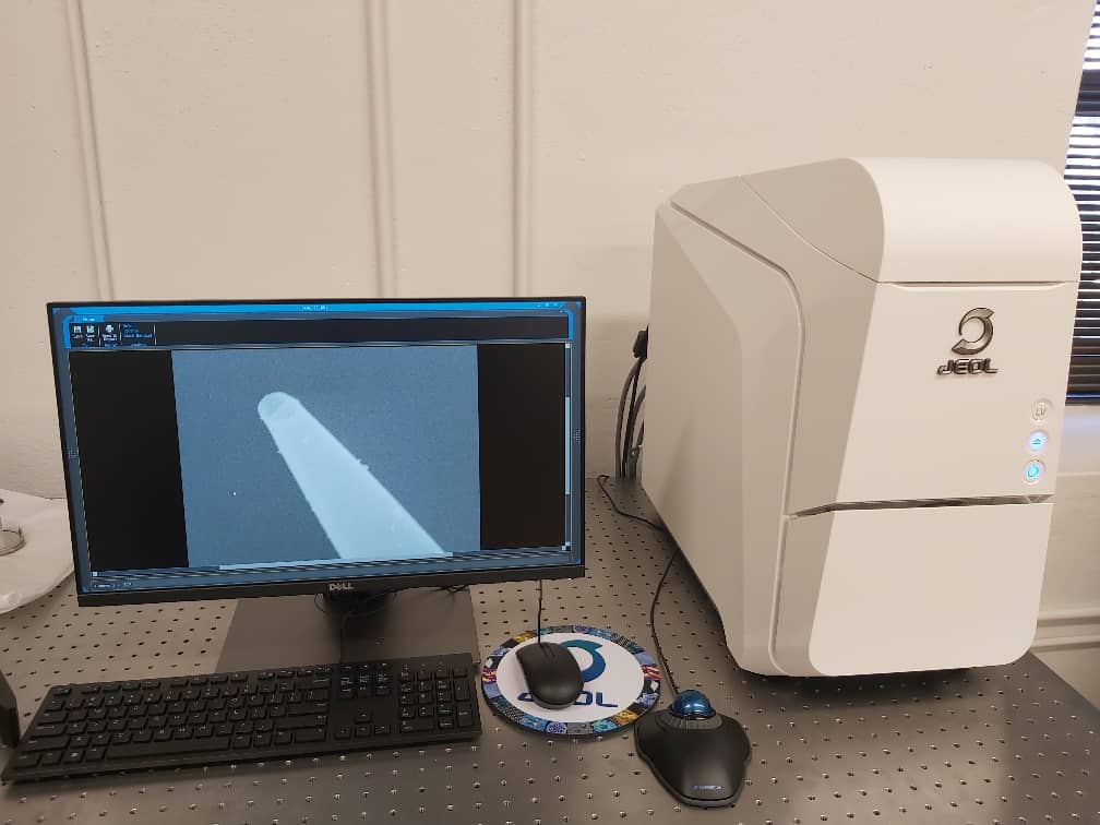
One of our most recent purchases is a NeoScope JCM-7000 benchtop scanning electron microscope (SEM) (JEOL, Japan) and we are super-excited about it.
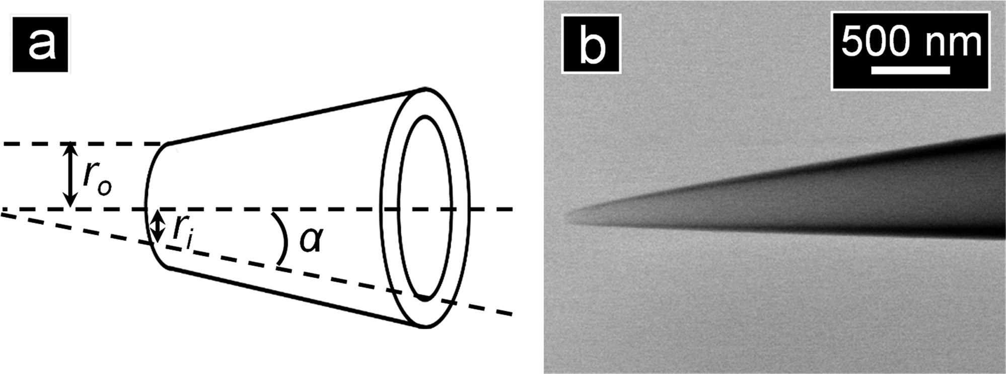
If asked what we’ll be imaging the most with this instrument, the answer will be nanopipets. Our group has demonstrated a vast range of applications for nanopipets e.g., SICM and SECCM imaging, sensing, electrodeposition, local nanoliter sampling, electrospray ionization, etc. For these applications, it is important to clearly characterize nanopipet geometry including the opening radius (ri), outer pipette tip opening radius (ro), and inner half-cone angle (α) of the tapered end.
These values go into the Finite Element Modeling simulations to understand experimental results and the electrochemical processes at and around nanopipets. While it is possible to get these dimensions with optical microscopy for large enough pipettes (e.g. 5-10 μm radii), electron microscopy is needed for nanopipets the sizes we often use – i.e., < 200 nm radius. Now, we can fabricate, use, and characterize our nanopipets, all in our lab without needing to travel across campus to use SEM in other facilities!
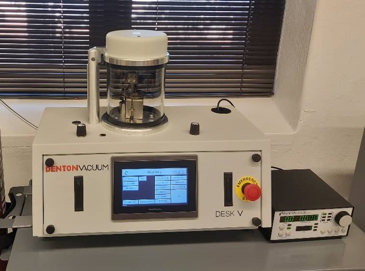
SEM characterization often requires the application of a conductive metal coating to reduce the charging of the glass nanopipette. So, to complete the set, we also acquired a DENTON sputter coater with quartz crystal microbalance (QCM) to deposit a thin layer of Au/Pd unto the borosilicate or quartz nanopipets before SEM imaging. The QCM allows monitoring of the thickness of the coating with sub-nanometer sensitivity.
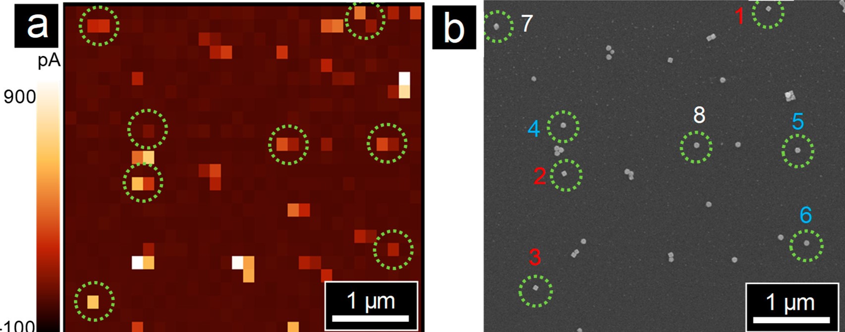
Aside from characterizing nanopipets, we can conveniently acquire electron micrographs of electrodes and substrates that we study with our electrochemical imaging techniques. This offers the possibility of directly correlating nanoscale structural details with electrochemical activity. With these instruments in our hub, we will surely develop new cool ways to incorporate them into our research projects!
